COMMU design/scematic error
-
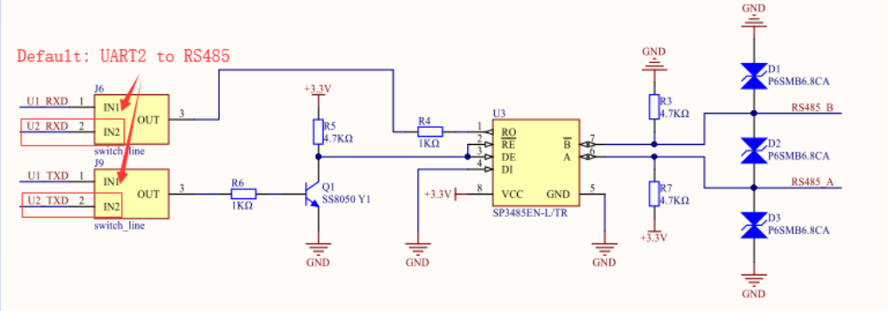
The RS485 interface design for the COMMU appears to be wrong. As shown, the transmit data (TXD) is used to enable/disable the driver on the DE/RE pins, while the driver data input, DI is permanently strapped low.
This means that sending data will drive a 'one' or float the line, but never drive a 'zero'.
The correct implementation should be TXD connected to the DI pin and a third signal used to control the DE/RE pins.
Since there is no third signal available, this design is fundamentally broken and won't interoperate with my existing systems.
V

Hello! It looks like you're interested in this conversation, but you don't have an account yet.
Getting fed up of having to scroll through the same posts each visit? When you register for an account, you'll always come back to exactly where you were before, and choose to be notified of new replies (either via email, or push notification). You'll also be able to save bookmarks and upvote posts to show your appreciation to other community members.
With your input, this post could be even better 💗
Register Login