M5 POWER BANK with IP5108
-
Under this link IP3506 AUTOMATIC STANDBY was discussed the M5 Power Bank module.
Here is the inspiration from the realization of this module:-
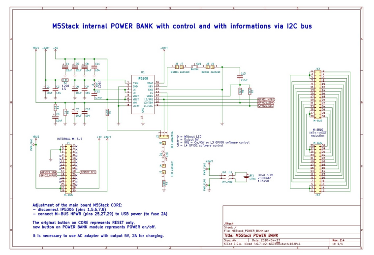
Schema
-
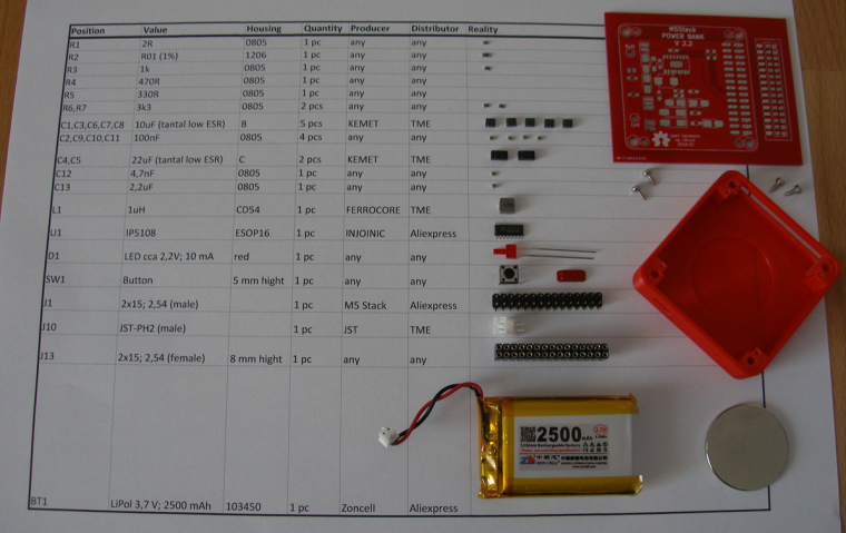
BOM
-
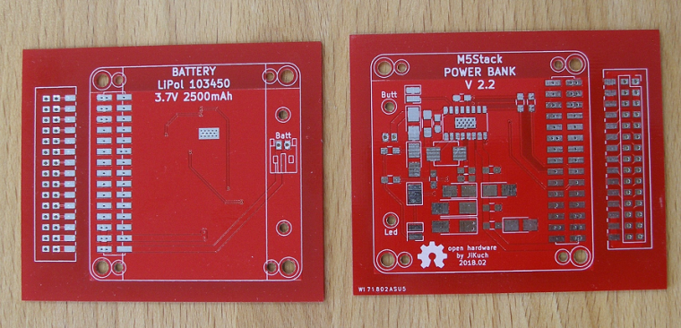
PCB for hand soldering
-
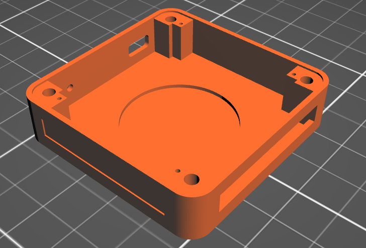
Case - 3D printed
-
Final functional module

M5 Power Bank with IP5108 fully replaces M5 BOTTOM:
- The module also contains a magnet (big one)
- External M-bus (fully) is on the right side (female 2x15)
- LED indicator and On/Off button is on the left side
- LED functionality can be selected (5V, On/Off=IRQ, GPIO00 or GPIO01 software control)
- On/Off button functionality can also be programmed thru IP5108 registers
WARNING:
The module is designed to be connected directly to the M5 CORE because the components enter the space of M5 CORE! -
-
Nice desing jikuch.... I am trying to adapt it for a solar powered system, but am unable to find information in english about the ip5108 i2c register.
Could you help me?
Thanks -
IP5108 I2C description:
7-bit slave address IP5108 is 0x75 (byte with write bit = 0xEA; byte with read bit = 0xEB)
400 Kbps speed of I2C supported
1 byte data = 8-bit data (bits from 7 to 0)WRITE Arduino example:
Wire.beginTransmission(0x75);
Wire.write(register_address_byte);
Wire.write(data_byte);
Wire.endTransmission();READ Arduino example:
Wire.beginTransmission(0x75);
Wire.write(register_address_byte);
Wire.endTransmission();
Wire.requestFrom(0x75,1);
data_byte = Wire.read();REGISTERS:
1. Enable / disable functions:
SYS_CTL0 = 0x01:- bit 4 (read/write): 0 = disbale / 1 = enable (1 = after reset) detection ??? (I do not understand.)
- bit 3 (read/write): 0 = disbale / 1 = enable (1 = after reset) light
- bit 2 (read/write): 0 = disbale / 1 = enable (1 = after reset) booster
- bit 1 (read/write): 0 = disable / 1 = enable (1 = after reset) charger
SYS_CTL1 = 0x02:
- bit 1 (read/write): 0 = disable / 1 = enable (1 = after reset) auto-standby
- bit 0 (read/write): 0 = disable / 1 = enable (1 = after reset) auto ??? (I do not understand.)
SYS_CTL3 = 0x03:
- bit 5 (read/write): 0 = disable / 1 = enable (1 = after reset) off by button
2. General setup features:
SYS_CTL2 = 0x0C:- bits 7-3 (read/write): (01010 = after reset) auto-standby current limit as multiple 12 mA
SYS_CTL4 = 0x04:
- bits 7-6 (read/write): (10 = after reset) time for auto-standby: 00=8s, 01=16s, 10=32s, 11=64s
SYS_CTL3 = 0x03:
- bits 7-6 (read/write): (01 = after reset) time for recognition button press: 00=1s, 01=2s, 10=3s, 11=4s
SYS_CTL5 = 0x07:
- bit 1 (read/write): (0 = after reset) control of light by button: 0=press, 1=double click
- bit 0 (read/write): (0 = after reset) off by button: 0=double click, 1=press
3. Charging setup features:
CHARGER_CTL1 = 0x22:- bits 3-2 (read/write): (01 = after reset) VOUT undervoltage limit during chargig: 00=4.53V, 01=4.63V, 10=4.73V, 11=4.83V
CHARGER_CTL2 = 0x24:
- bits 6-5 (read/write): (00 = after reset) battery type = charging voltage: 00=4.2V, 01=4.3V, 10=4.35V
- bits 2-1 (read/write): (10 = after reset) overcharging of charging: 00=0mV, 01=14mV, 10=28mV, 11=42mV
CHG_DIG_CTL4 = 0x25:
- bits 4-0 (read/write): (10110 = after reset) charging current setting [A]:
b0 x 0.1 + b1 x 0.2 + b2 x 0.4 + b3 x 0.6 + b4 x 1.4
4. Charging information:
Reg_READ0a = 0x70:- bit 3 (read only): charging status: 0 = not charging, 1 = charging
Ref_READ0b = 0x71:
- bits 7-5 (read only): detailed charging status:
000 = inactivity
001 = charging
010 = constant current charging
011 = charging with constant voltage
100 = ??? (missing description in original document)
101 = end of charging (maintenance current) - bit 3 (read only): signal of end of charging (=1)
5. PIN assignment & control:
MFP_CTL0 = 0x51:- bits 5-4 (read/write): (00 = after reset) pin LIGHT assignement: 00=WLED, 01=GPIO2, 10=VREF
- bits 3-2 (read/write): (00 = after reset) pin L4 assignement: 00=L4, 01=GPIO1
- bits 1-0 (read/write): (00 = after reset) pin L3 assignement: 00=L3, 01=GPIO0
GPIO_CTL2a = 0x53:
- bits 2-0 (read/write): (000 = after reset) GPIO[2:0] input enable
GPIO_CTL2b = 0x54:
- bits 2-0 (read/write): (000 = after reset) GPIO[2:0] output enable
GPIO_CTL3 = 0x55:
- bits 2-0 (read/write): (000 = after reset) GPIO[2:0] data
6. Measurement:
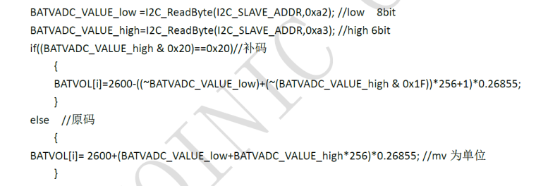
BATVADC_DAT0 = 0xA2:- pins 7-0 (read only): LOW 8 bits (byte) of BATVADC
BATVADC_DAT1 = 0xA3:
- pins 5-0 (read only): HIGH 6 bits of BATVADC
Calculation according to the original document:
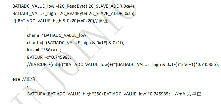
BATIADC_DAT0 = 0xA4:
- pins 7-0 (read only): LOW 8 bits (byte) of BATIADC
BATIADC_DAT1 = 0xA5:
- pins 5-0 (read only): HIGH 6 bits of BATIADC
Calculation according to the original document:
BATOCV_DAT0 = 0xA8:
- pins 7-0 (read only): LOW 8 bits (byte) of BATOCV
BATOCV_DAT1 = 0xA9:
- pins 5-0 (read only): HIGH 6 bits of BATOCV
Calculation according to the original document:
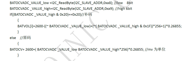
This is true: BATOCV = BATVACD + BATIADC * battery_internal_resistnace
7. WLED status:
Reg_READ1 = 0x72:- bit 7 (read only): 0 = WLED is off, 1 = WLED is on
8. Light / heavy load:
Reg_READ1 = 0x72:- bit 6 (read only): 0 = heavy load over 75 mA, 1 = light load less 75 mA
9. Button control:
Reg_READ2 = 0x77:- bit 3 (read; write 1 = reset) flag button double clicked (=1)
- bit 1 (read; write 1 = reset) flag button pressed (=1)
- bit 0 (read; write 1 = reset) flag button clicked (=1)
That is all.
-
@jikuch Nice design.
Do you have the I2C register document of IP5108? Could you share it? Thanks! -
Hi, can somebody tell me: if I change something in ip5108 through i2c, will it be saved, or i must make this changes each time when i start device?
-
Hi, can you tell me: if I change something in ip5108 through i2c (for example disable auto-standby), will this changers be saved, or i must make this changes (with software) each time when i start device?
Hello! It looks like you're interested in this conversation, but you don't have an account yet.
Getting fed up of having to scroll through the same posts each visit? When you register for an account, you'll always come back to exactly where you were before, and choose to be notified of new replies (either via email, or push notification). You'll also be able to save bookmarks and upvote posts to show your appreciation to other community members.
With your input, this post could be even better 💗
Register Login